- 您现在的位置:买卖IC网 > Sheet目录364 > SST25WF040-40-5I-QAE-T (Microchip Technology)IC FLASH SER 4MB 40MHZ SPI 8WSON
�� �
�
�512� Kbit� /� 1� Mbit� /� 2� Mbit� /� 4� Mbit� 1.8V� SPI� Serial� Flash�
�A� Microchip� Technology� Company�
�SST25WF512� /� SST25WF010� /� SST25WF020� /� SST25WF040�
�Data� Sheet�
�Pin� Description�
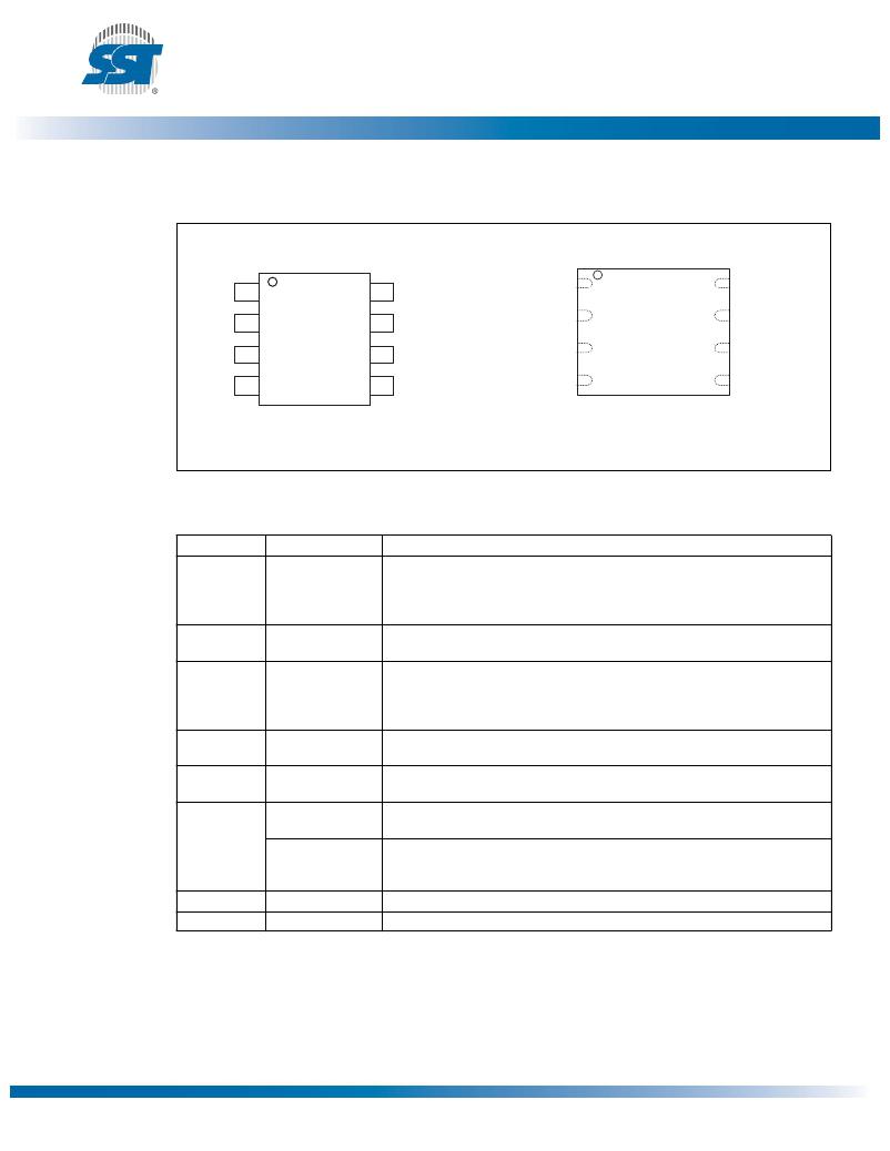
�Top� View�
�CE#�
�1�
�8�
�V� DD�
�CE#�
�1�
�8�
�VDD�
�SO�
�WP#�
�V� SS�
�2�
�3�
�4�
�7�
�6�
�5�
�RST#/HOLD#�
�SCK�
�SI�
�SO�
�WP#�
�VSS�
�2�
�3�
�4�
�Top� View�
�7�
�6�
�5�
�RST#/HOLD#�
�SCK�
�SI�
�1328� 08-wson� P2.0�
�1328.25WF� 08-soic-P0.0�
�8-Lead� SOIC�
�8-Contact� WSON�
�Figure� 2:� Pin� Assignment� for� 8-Lead� SOIC� and� 8-Contact� WSON�
�Table� 1:� Pin� Description�
�Symbol�
�SCK�
�SI�
�Pin� Name�
�Serial� Clock�
�Serial� Data� Input�
�Functions�
�To� provide� the� timing� of� the� serial� interface.�
�Commands,� addresses,� or� input� data� are� latched� on� the� rising� edge� of� the�
�clock� input,� while� output� data� is� shifted� out� on� the� falling� edge� of� the� clock�
�input.�
�To� transfer� commands,� addresses,� or� data� serially� into� the� device.�
�Inputs� are� latched� on� the� rising� edge� of� the� serial� clock.�
�SO�
�Serial� Data� Output� To� transfer� data� serially� out� of� the� device.�
�Data� is� shifted� out� on� the� falling� edge� of� the� serial� clock.�
�Flash� busy� status� pin� in� AAI� mode� if� SO� is� configured� as� a� hardware� RY/BY#�
�pin.� See� “End-of-Write� Detection”� on� page� 16.� for� more� information.�
�CE#�
�WP#�
�RST#/�
�HOLD#�
�V� DD�
�V� SS�
�Chip� Enable�
�Write� Protect�
�Reset�
�Hold�
�Power� Supply�
�Ground�
�The� device� is� enabled� by� a� high� to� low� transition� on� CE#.� CE#� must� remain�
�low� for� the� duration� of� any� command� sequence.�
�The� Write� Protect� (WP#)� pin� is� used� to� enable/disable� BPL� bit� in� the� status�
�register.�
�To� reset� the� operation� of� the� device� and� the� internal� logic.� The� device� powers�
�on� with� RST#� pin� functionality� as� default.�
�To� temporarily� stop� serial� communication� with� SPI� Flash� memory� while�
�device� is� selected.� This� is� selected� by� an� instruction� sequence� which� is�
�detailed� in� “Reset/Hold� Mode”� on� page� 6.�
�To� provide� power� supply� voltage:� 1.65-1.95V� for� SST25WF512/010/020/040�
�T1.0� 25016�
�?2011� Silicon� Storage� Technology,� Inc.�
�4�
�DS25016A�
�06/11�
�发布紧急采购,3分钟左右您将得到回复。
相关PDF资料
SST25WF080-75-4I-ZAE
IC FLSH SER 8MB 75MHZ SPI 8CSP
SST26VF032A-80-5I-S2AE
IC FLASH 32MBIT 8SOIC
SST38VF6402-90-5I-B3KE-T
IC FLASH MPF 64MBIT 90NS 48TFBGA
SST39LF802C-55-4C-MAQE-T
IC FLASH MPF 8MBIT 48-WFBGA
SST39SF040-70-4C-WHE
IC FLASH MPF 4MBIT 70NS 32TSOP
SST39VF1602C-70-4I-B3KE
IC FLASH MPF 16MBIT 70NS 48TFBGA
SST39VF200A-70-4I-MAQE
IC FLASH MPF 2MBIT 70NS 48-WFBGA
SST39VF3201-70-4I-B3KE-T
IC FLASH MPF 32MBIT 70NS 48TFBGA
相关代理商/技术参数
SST25WF040-40-5I-QAF
制造商:SST 制造商全称:Silicon Storage Technology, Inc 功能描述:512 Kbit / 1 Mbit / 2 Mbit / 4Mbit 1.8V SPI Serial Flash
SST25WF040-40-5I-SAE
制造商:SST 制造商全称:Silicon Storage Technology, Inc 功能描述:512 Kbit / 1 Mbit / 2 Mbit / 4Mbit 1.8V SPI Serial Flash
SST25WF040-40-5I-SAF
功能描述:闪存 4M (512Kx8) 40MHz Industrial Temp RoHS:否 制造商:ON Semiconductor 数据总线宽度:1 bit 存储类型:Flash 存储容量:2 MB 结构:256 K x 8 定时类型: 接口类型:SPI 访问时间: 电源电压-最大:3.6 V 电源电压-最小:2.3 V 最大工作电流:15 mA 工作温度:- 40 C to + 85 C 安装风格:SMD/SMT 封装 / 箱体: 封装:Reel
SST25WF040-40-5I-SAF-T
功能描述:闪存 1.65 to 1.95V 4Mbit SPI Serial 闪存 RoHS:否 制造商:ON Semiconductor 数据总线宽度:1 bit 存储类型:Flash 存储容量:2 MB 结构:256 K x 8 定时类型: 接口类型:SPI 访问时间: 电源电压-最大:3.6 V 电源电压-最小:2.3 V 最大工作电流:15 mA 工作温度:- 40 C to + 85 C 安装风格:SMD/SMT 封装 / 箱体: 封装:Reel
SST25WF080
制造商:SST 制造商全称:Silicon Storage Technology, Inc 功能描述:8Mbit 1.8V SPI Serial Flash
SST25WF080_12
制造商:MICROCHIP 制造商全称:Microchip Technology 功能描述:8 Mbit 1.8V SPI Serial Flash
SST25WF080-75-4I-SAE
制造商:SST 制造商全称:Silicon Storage Technology, Inc 功能描述:8Mbit 1.8V SPI Serial Flash
SST25WF080-75-4I-SAF
功能描述:闪存 8M (1Mx8) 75MHz Industrial Temp RoHS:否 制造商:ON Semiconductor 数据总线宽度:1 bit 存储类型:Flash 存储容量:2 MB 结构:256 K x 8 定时类型: 接口类型:SPI 访问时间: 电源电压-最大:3.6 V 电源电压-最小:2.3 V 最大工作电流:15 mA 工作温度:- 40 C to + 85 C 安装风格:SMD/SMT 封装 / 箱体: 封装:Reel